The TS-520 and 820 series and many others made by Kenwood, Yaesu and others can be improved to give better IMD and tube life by changing a few components and adding a new screen grid supply circuit.
We will cover the modifications is several stages and the reader may then decide the best approach when modifying their transceiver.
Note: No guarantee can be given as the suitability of these modifications, they work on my TS-520 and TS-820S, and your experience may be different. Therefore the onus is on the modifier as to whether the results will be same as I experienced.
Stage 1
Many HF transceivers equipped with the 6146 and 6SJ6C series of valves/tubes are not optimised for linearity and reliable operation. Almost all of these transceivers use an unregulated screen grid supply. Because of this the biasing of the tubes varies over the RF envelope when operating on SSB. The manufacturers of the valves/tubes normally recommend a certain minimum resistance is connected in series with the screen grid to limit the peak current and the supply should be adequately stabilised. If the screen grid current is exceeded the tube life is reduced. If excessive screen grid current flows the tube can be destroyed in a very short time, as little as 5s in some cases!
Taking the popular 6146 series of tubes as an example. The maximum safe screen grid current when the maximum allowed screen grid voltage is applied is only 8mA per tube. The manufacturers absolute maximum screen voltage for the tube is +250V, but it is recommended it should not exceed +200V for best tube life and reliability when driven to maximum output.
Many HF transceivers examined seem to ignore these factors and often these cause tube failures, with attendant other damage and expense. So we will start by examining the components in the PA of the TS-820. The comments apply equally well to many other makes and models.
The picture below shows the view looking into the tube base compartment of my TS-820S.
Earlier Kenwood transceivers did not use a printed circuit board to hold the tube bases and other components, they used point to point wiring for the various components. The PCB approach allows easier maintenance and a neater looking finished product.
One thing you should check before proceeding is the tightness of the screws holding the tube board to the chassis. These screws conduct the DC and RF current to ground. If the contact is suspect instability and erratic operation may occur.
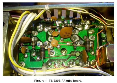
In the picture can be seen two large resistors and two smaller ones, as well as several capacitor and other components. The two large resistors are the cathode current metering resistors and these develop a voltage across them when the anode current flows. In fact the current measured is the sum of the anode and screen grid current. This voltage is used to drive the IP meter showing anode current. (The IP meter calibration resistor is adjacent to the left cathode resistor connecting to point IPM). Because the cathodes have been raised above ground this is a form of RF negative feedback and this will lower the gain. To correct this the cathodes are shunted by several disc ceramic decoupling capacitors to hold the cathodes at RF ground.
The large resistors in the TS-820 series (and many other Kenwood transceivers) are 10Ω / 1W carbon composition types. These change their value over time especially if the resistor gets hot, which it does in a high power RF amplifier. Therefore it is very common to find the resistors when measured with an ohm meter are as much as 50% higher in value than the marked value.
This causes the IP meter to read higher than the actual anode current flowing and so we have to increase the grid bias voltage to bring the idle current back to the correct value. In the TS-820 this is 60mA. But if the cathode resistors have gone higher in value by 50% this means the actual idle current is only about 40mA and this affects the linearity and gain! If a tube suffered a flash-over or other internal failure the cathode resistors can be blown open circuit due to the high current flowing and this allows the full anode voltage to be applied to the IP meter resistor. Measure all the resistors in circuit with an ohmmeter to establish if they within specification.
A very good idea is to change the cathode resistors for something more suited to high peak currents and temperature. I normally replace them with 10Ω / 5W wire-wound resistors. The physical size of a 5W wire-wound resistor is almost the same so no difficulty arises.
Turning now to the two smaller resistors seen in the picture. These are 100Ω / 1/4W carbon composition resistors in series with the screen grid and the supply. These act as "antiparasitic" stopper resistors to reduce the tendency of the tubes to oscillate at some high frequency. They are shunted at the screen grid pin by decoupling capacitors to hold the screen grid at zero RF voltage.
Because the screen grid supply is not stabilised but simply a half-wave rectifier with a large value electrolytic capacitor it can support quite high peak currents for short periods. RCA and other who manufacture the 6146 and similar tubes recommend that a resistor of at least 1kΩ be connected in series with the screen grid pin and the stabilised supply to limit the peak screen grid current to safe levels. However, even if the screen supply is stabilised this high value of series resistor causes a voltage drop across the series resistor and the gain to fall as the screen grid current rises. With a 1kΩ resistor and a peak screen grid current of 8mA this is a voltage variation of 8V, which is quite poor. If the screen grid voltage is 200V then as a percentage this is 4% variation. So the linearity at high drive level becomes very poor and the way the manufacturers counteract this is to ignore the recommendation and allow the screen grid current to rise to dangerous levels.
If the screen grid stopper resistors are measured they are very often much higher in value than the 100Ω they are supposed to be. Part of this is normal aging, these transceivers are now about 20 years or more in age, the remainder is because they have been severely over-dissipated by the high peak screen currents allowed to flow because the supply has virtually no current limiting. In my TS-820S when I purchased the transceiver secondhand one measured almost 200Ω and the other was about 160Ω. Hence, a very good modification is to replace them with something higher in rating and better quality.
I normally use 2W wire-wound resistors (which are about the same size as the 1/4W carbon composition types) for a good margin of safety. The extra inductance is actually a benefit in suppressing parasitic oscillation.
Stage 2
Because the linearity heavily depends on the screen grid supply being a constant voltage we need to devise a way to hold the screen grid voltage to something more constant with changing screen grid current. The unregulated rectified supply voltage varies as the AC mains voltage goes up and down and as current is drawn from the supply.
In my TS-520 before it was modified I measured the offload voltage as being almost +300V on the nominal +210V rail that feeds the screen grids of the 6146's. Under full drive it fell to about +190V. This is a variation of almost 100V between no drive and full drive and the IMD was quite poor. After modification the IMD improved by 10dB at full output and considerably more at lower drive levels. The RF output power remained the same as before.
One method is to utilise a type of voltage stabiliser. We could make a voltage regulator using a high voltage series pass transistor and feed the output of this to the screen grids. However, a word of warning about series regulators. Under certain parts of the RF drive cycle the anode voltage swings down towards ground. If the anode voltage swings lower than the voltage applied to the screen grid then the screen grid tries to take over the function of the anode and it experiences high screen current flowing into the tube. If the screen grid voltage has been raised above the recommended value of +200V then the screen grid voltage is closer to the anode voltage and the screen grid current will begin rising sooner when the anode voltage approaches it. Hence, raising the screen grid voltage is wrong, if anything we should be lowering it allow a greater anode voltage swing, which equates to more power output.
I know this sounds wrong but it is true and examining the tube characteristic curves will highlight this fact. In general a 6146 needs only about +150V screen voltage to deliver its maximum rated power and somewhere between +150V and +175V is a good choice. I run my TS-520 with a screen grid voltage of +150V and I obtain 130W pep on 80 and 40m, 100W pep on 20m and about 80W pep on 10m. No significant increase in output power is obtained with +200V screen grid voltage, at best a few watts.
When the anode voltage is swinging upwards on the opposite half cycle of the RF envelope the opposite effect occurs. Now the rising anode voltage is being used to force current out of the tube via the screen grid and this is "negative screen current". If a series stabiliser is used under the positive screen current condition the voltage can be held to the correct value. If a series resistor is included in series with the input to the pass transistor we can also limit the peak screen current. The basis of a simple high voltage stabiliser is shown in this circuit..
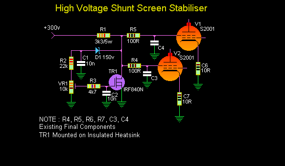 The mosfet is mounted on a heatsink with an insulating film between the drain tab and the
metal plate. The zener diode D1 is a 1W type made up from two 75V diodes connected in
series. Resistor R1 is the dropper resistor and needs to be adequately rated for dissipation.
In this application a 5 to 10W wire-wound is the best choice. R2 is a 1/4W metal film or
carbon film resistor. VR1 is a 1/2W printed circuit board type. Capacitor C1 needs to be at
least a 250V rating, C2 can be a 50V type ceramic disc or similar. The components R4, R5,
R6, C3 & C4 are the existing ones around the 6146 tubes fitted by the manufacturer of the
HF transceiver.
The mosfet is mounted on a heatsink with an insulating film between the drain tab and the
metal plate. The zener diode D1 is a 1W type made up from two 75V diodes connected in
series. Resistor R1 is the dropper resistor and needs to be adequately rated for dissipation.
In this application a 5 to 10W wire-wound is the best choice. R2 is a 1/4W metal film or
carbon film resistor. VR1 is a 1/2W printed circuit board type. Capacitor C1 needs to be at
least a 250V rating, C2 can be a 50V type ceramic disc or similar. The components R4, R5,
R6, C3 & C4 are the existing ones around the 6146 tubes fitted by the manufacturer of the
HF transceiver.Note that C1 and C2 are fitted for RF decoupling reasons to stop RF upsetting the regulator. Do not increase these in value, as this will slow down the response of the regulator to the rapidly changing current drawn by the screen grids.
The IRF840 mosfet is a TO-220 type rated at 500V drain-source and a drain dissipation of about 60W when correctly heatsinked. Many other types can be used as long as the drainsource voltage rating is at least 300V.
Using this circuit in my TS-520 I measured a maximum variation in the screen grid voltage of about 20mV between zero drive and full drive and the IMD improved noticeably at full power output. As long as the input-output voltage differential is above 20V the regulator performs satisfactorily, hence in many cases the nominal +210V rail can be used.
A further improvement in IMD can also be obtained by feeding the driver tube (12BY7A) screen grid from a similar shunt stabiliser. In the original design this is fed from the +210V rail with a dropper resistor and a shunt resistor. This voltage also varies with RF drive level and a simple method would be a 1W or higher zener to replace the shunt resistor with a change in the series resistor to ensure enough screen current is available on speech peaks. In my TS-520 I use the same shunt regulator that feeds the PA tubes to feed the 12BY7A screen grid via a dropper resistor.
Installing Screen Grid Regulator
There are a number of problems when we want to include a shunt regulator in the TS-520 and 820 transceivers and I suspect similar other Kenwood models although I have no experience with these. The inclusion of a screen regulator without losing some of the functions requires us to connect the regulator in the correct part of the wiring and change a number of components to increase reliability over and above the ones already mentioned.
In order to understand the problem I have drawn Figure 5 and 6. Figure 5 shows the way the screen grid is supplied normally and also when the SG switch on the rear panel is set to the OFF position.
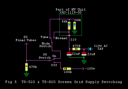
Figure 5 TS-520 and 820 screen grid supply switching
The nominal +210V to feed the screen grid is derived from a tap on the main high voltage transformer and half wave rectified. Two 22μF/450V electrolytic capacitors with a 470Ω resistor smooth the DC. The front panel MODE switch has several wafers and one is used for switching in an extra resistor potential divider when the TUNE position is selected.
Two 56kΩ resistors mounted on the HV Unit board serve to drop the screen grid voltage to half the normal value. This limits the anode current when tuning up initially. When the MODE switch is moved to any position other than TUNE the screen grid receives the full +210V supply rail.
The SG switch on the rear panel is used for aligning the transceiver and also when the transverter facility is used. When the SG switch is set to OFF the tube screen grids are connected to a -100V supply via a 100kΩ resistor. This ensures the tubes are fully cut-off.
One component missing is the 470kΩ resistor across the screen grid supply. This is a safety resistor should the SG switch be only partially switched it is possible for both the -100V and the +210V supply to be disconnected and then the screen grids would be left floating. Without the 470kΩ resistor they can float up to the anode voltage and this can cause a flashover in the tubes.
It is strongly recommended this resistor be fitted even if you do not make any other modifications.
It can be a 1/2W metal film or carbon film type.
If we now examine Figure 6 you will see the correct position for the screen grid regulator and the other changes needed to the wiring and components.
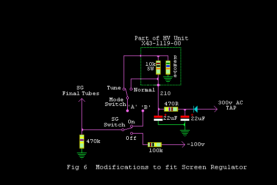
Figure 6 Modifications to fit screen regulator
The simplest way to connect the shunt regulator is to lift the wire from the SG switch that runs from the MODE switch and to connect this to the input of the shunt regulator. (In my TS-820S this is a brown wire, but check yours with a voltmeter to be certain). From the output of the regulator we run a wire to the SG terminal where we disconnected the original wire. These are shown in Figure 6 as A and B. To correct the TUNE function we need to remove the grounded 56kΩ resistor and change the other to a 10kΩ / 5W wire-wound.
There is just enough room on the HV Unit board to do this. Alternatively connect two 4k7Ω / 2W wire-wound resistors in series and fit in place of the original 56kΩ resistor.
Finally, we can move the 210V rectifier feed from the normal tap on the transformer to the 300V tap. If the screen grid voltage is adjusted to +175V, which is a good compromise between power output and good IMD, then the normal +210V nominal supply is sufficient. If you want a bit more screen grid voltage then we need to raise the regulator input voltage.
In my TS-820S the 210V rectifier is connected to the 230V tap on the secondary and the wire is green. The 300V tap has an orange wire to the rectifier board. The 210V and 300V AC input pins are adjacent so a simple way is the remove the green wire altogether and to link the 210 and 300 pins.
The advantage of this modification is that once the idle current has been set to 60mA it will remain correctly biased right up to full anode current, which it doesn't, in the standard circuit!
This is because when the bias pot is adjusted the screen grid voltage is abnormally high and the screen grid voltage falls as the anode current and the screen current increases so moving the biasing more towards Class-C. When TUNE is selected the screen grid voltage is +200V when no drive is used and as the drive is increased the voltage falls to a lower level because of the extra 10kΩ resistor connected in series with the input to the regulator causes a voltage drop.
Stage 3 Alternative output tubes
The Kenwood TS-520 and 820 series used the S-2001A pentode, which are direct equivalents of the RCA 6146A. Many other tube types will work with equal performance. The tube I favour is a different type but a near drop in replacement. It is the 12V heater version of the 6146A, type number 6883B / 8032A / 8552 made by RCA and others. Its RF characteristics are identical to the 6146A except for the heater voltage.
To change to the 12V version we need to make a slight wiring change to the tube base board. The S-2001A / 6146A tubes have the 6V heaters wired in series and connected to the 12V AC winding of the transformer. We need to change the wiring so the tubes are now connected in parallel and both fed with 12V AC. On the tube board is a link wire from one heater pin to the other tube heater pin. Remove this link wire and solder a short piece of wire from this pin to ground. Run a new piece of wire from the second tube base to the 12V AC input.
The heater current of the two parallel connected 12V heater tubes is the same as the two 6146s connected in series. The advantage of the 12V heater version is that they are more tolerant to mains voltage variations because they were designed for use in 12V automotive fed transmitters, where the battery voltage limits are about 11V to 15V.
Another modification I have recently become aware of is the use of the 6293 tube. I am strongly against this modification for several reasons. The 6293 tube was designed by RCA as a high current pulse modulator. Physically it is identical to the 6146 series, uses the same heater voltage and the pin out is identical, so they can be dropped in without any changes. The problem is the recommended modification doesn't appreciate the subtle difference between a pulse modulator and a tube intended for SSB or CW operation.
The 6293 is able to handle much higher anode current peaks, about 10-times that of a 6146, but only for a very short duration. If the RCA data on the 6293 is studied carefully they state that the maximum anode pulse is limited to 10μs with a duty cycle not exceeding 1%.
SSB and CW operation duty cycle is about 30 to 40% on average and the anode current is quite high on the peaks, much more than the IP meter indicates because this is heavily damped and cannot follow rapidly changing current. It indicates the "average current" which is only about 60% of the actual value when SSB or CW is used. Under normal operation the peak anode current is about 2-times the value the IP meter shows.
The official safe anode dissipation of the 6293 is obtained from the duty cycle graph RCA supplied in the data sheet. At 1% maximum duty cycle the safe anode dissipation is only 10W. The 6146 and its variants have an anode dissipation of ≈30W under ICAS duty and 20W under the CCS rating.
The other disturbing fact is the raising of the screen grid supply from the original nominal +210V supply rail, which in normal operation is closer to +250V, to the +300V supply rail. This supply off load is about +350V or higher and only falls to about +320V under full load. Although RCA give a maximum screen voltage of +350V for the 6293 tube this value is for pulse operation, RCA recommend that equipment manufacturers limit the screen voltage to +200V, the same as the 6146A, so they are quite similar and almost identical safe screen dissipation values. In fact the major difference between the two types is the cathode structure, this can supply more electrons, hence higher peak anode currents, but only for very low duty cycle service.
In the modification schedule the grid bias needs to be raised to cater for the higher screen grid voltage and this compounds the IMD degradation. The claim in the modification sheet is that the RF output almost doubles, but no mention is made about what happens to the IMD performance!
The reason the modification is made is stated to be because some external linear amplifiers are unable to be driven to full output with a standard TS-820 without the modification. In cascaded linear amplifier stages - such as a HF transceiver driving a linear amplifier - the resultant IMD performance is a combination of the two stages connected in series.
In general a good rule of thumb is that if the final signal needs to be, say, -26dBc for the third order IMD products then the driver IMD needs to be approx 6dB better to achieve this figure, a figure of -32dBc. The standard TS-520 and 820 series (and many others using a similar tube line up) gives at best about -24dBc at 100W pep output. With a good screen grid stabiliser this can rise to as high as -34dBc at the same power output, hence less splatter on the bands!
It must not be forgotten that the high voltage transformer fitted to the TS-520 and 820 series transceivers is a limited rating and can only supply a certain current before it begins to saturate. If an attempt is made to draw too much current it will overheat and probably fail.
The high voltage rectifier diodes used for the +900V anode supply are also a little on the light side for the required peak currents because the smoothing system is a capacitor input filter and the diode peak currents are about 4-times the average output current. In my personal opinion the TS-520 and 820 anode voltage supply and transformer is about on its safe limit even under normal operation as designed.